- 您现在的位置:买卖IC网 > Sheet目录1997 > ICS810001DK-21LFT (IDT, Integrated Device Technology Inc)IC CLK GEN SYNC VCXO DL 32VFQFN
ICS810001DK-21 REVISION B APRIL 13, 2010
8
2010 Integrated Device Technology, Inc.
ICS810001-21 Data Sheet
FEMTOCLOCK DUAL VCXO VIDEO PLL
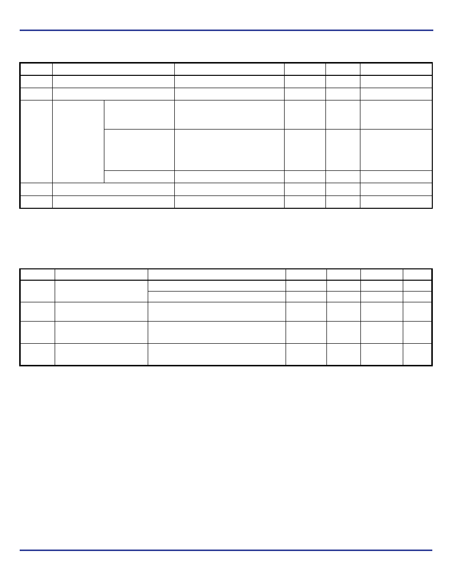
Table 4B. LVCMOS/LVTTL DC Characteristics, VDD = VDDO = VDDX = 3.3V ± 5%, TA = 0°C to 70°C
AC Electrical Characteristics
Table 5. AC Characteristics, VDD = VDDO = VDDX = 3.3V ± 5%, TA = 0°C to 70°C
NOTE: Electrical parameters are guaranteed over the specified ambient operating temperature range, which is established when the device is
mounted in a test socket with maintained transverse airflow greater than 500 lfpm. The device will meet specifications after thermal equilibrium
has been reached under these conditions.
See Parameter Measurement Information Section.
NOTE 1: Refer to the Phase Noise Plot.
NOTE 2: Lock Time measured from power-up to stable output frequency.
Symbol
Parameter
Test Conditions
Minimum
Typical
Maximum
Units
VIH
Input High Voltage
2.0
VDD + 0.3
V
VIL
Input Low Voltage
-0.3
0.8
V
IIH
Input
High Current
CLK[0:1], CLK_SEL,
P[1:0], V[3:0], N[1:0],
MR, MF, XTAL_SEL
VDD = VIN = 3.465V
150
A
OE, nBP0, nBP1
VDD = VIN = 3.465V
5
A
IIL
Input
Low Current
CLK[0:1], CLK_SEL,
P[1:0], V[3:0], N[1:0],
MR, MF, XTAL_SEL
VDD = 3.465V, VIN = 0V
-5
A
OE, nBP0, nBP1
VDD = 3.465, VIN = 0V
-150
A
VOH
Output High Voltage
IOH = -24mA
2.6
V
VOL
Output Low Voltage
IOL = 24mA
0.5
V
Symbol
Parameter
Test Conditions
Minimum
Typical
Maximum
Units
fOUT
Output Frequency
nBP0, nBP1 = 00
14
35
MHz
nBP1 = 1
31
175
MHz
tjit()
RMS Phase Jitter, (Random),
NOTE 1
148.3516MHz,
Integration Range: 12kHz – 20MHz
1.089
ps
tR / tF
Output Rise/Fall Time
20% to 80%
250
750
ps
odc
Output Duty Cycle
48
52
%
tLOCK
VCXO & FemtoClock PLL
Lock Time; NOTE 2
M = 92, Bandwidth = 475Hz
100
ms
M = 4004, Bandwidth = 6Hz
25
s
发布紧急采购,3分钟左右您将得到回复。
相关PDF资料
ICS81006AKLFT
IC VCXO TO 6 LVCMOS OUT 20VFQFPN
ICS810525AGILF
IC VCXO-LVCMOS/LVTTL 16-TSSOP
ICS813076CYILF
IC VCXO-PLL WIRELESS 64-TQFP
ICS813078BYILF
IC VCXO PLL WIRELESS 64TQFP
ICS813323BGLF
IC ATTENUATOR/MULTIPLIER 24TSSOP
ICS840002AGLF
IC FREQ SYNTHESIZER 16-TSSOP
ICS840022AKI-02LF
IC CLOCK GENERATOR 16VFQFPN
ICS84021AYLF
IC SYNTHESIZER HIGH FREQ 32-LQFP
相关代理商/技术参数
ICS810-06
制造商:ICS 制造商全称:ICS 功能描述:VCXO-TO-6 LVCMOS OUTPUTS
ICS81006AK
制造商:ICS 制造商全称:ICS 功能描述:VCXO-TO-6 LVCMOS OUTPUTS
ICS81006AKI
制造商:ICS 制造商全称:ICS 功能描述:VCXO-TO-6 LVCMOS OUTPUTS
ICS81006AKILF
功能描述:IC VCXO TO 6 LVCMOS OUT 20VFQFPN RoHS:是 类别:集成电路 (IC) >> 时钟/计时 - 时钟发生器,PLL,频率合成器 系列:HiPerClockS™ 标准包装:1,000 系列:- 类型:时钟/频率合成器,扇出分配 PLL:- 输入:- 输出:- 电路数:- 比率 - 输入:输出:- 差分 - 输入:输出:- 频率 - 最大:- 除法器/乘法器:- 电源电压:- 工作温度:- 安装类型:表面贴装 封装/外壳:56-VFQFN 裸露焊盘 供应商设备封装:56-VFQFP-EP(8x8) 包装:带卷 (TR) 其它名称:844S012AKI-01LFT
ICS81006AKILFT
功能描述:IC VCXO TO 6 LVCMOS OUT 20VFQFPN RoHS:是 类别:集成电路 (IC) >> 时钟/计时 - 时钟发生器,PLL,频率合成器 系列:HiPerClockS™ 标准包装:1,000 系列:- 类型:时钟/频率合成器,扇出分配 PLL:- 输入:- 输出:- 电路数:- 比率 - 输入:输出:- 差分 - 输入:输出:- 频率 - 最大:- 除法器/乘法器:- 电源电压:- 工作温度:- 安装类型:表面贴装 封装/外壳:56-VFQFN 裸露焊盘 供应商设备封装:56-VFQFP-EP(8x8) 包装:带卷 (TR) 其它名称:844S012AKI-01LFT
ICS81006AKIT
制造商:ICS 制造商全称:ICS 功能描述:VCXO-TO-6 LVCMOS OUTPUTS
ICS81006AKLF
功能描述:IC VCXO LOW PHASE NOISE 20-VFQFN RoHS:是 类别:集成电路 (IC) >> 时钟/计时 - 时钟发生器,PLL,频率合成器 系列:HiPerClockS™ 标准包装:2,000 系列:- 类型:PLL 频率合成器 PLL:是 输入:晶体 输出:时钟 电路数:1 比率 - 输入:输出:1:1 差分 - 输入:输出:无/无 频率 - 最大:1GHz 除法器/乘法器:是/无 电源电压:4.5 V ~ 5.5 V 工作温度:-20°C ~ 85°C 安装类型:表面贴装 封装/外壳:16-LSSOP(0.175",4.40mm 宽) 供应商设备封装:16-SSOP 包装:带卷 (TR) 其它名称:NJW1504V-TE1-NDNJW1504V-TE1TR
ICS81006AKLFT
功能描述:IC VCXO TO 6 LVCMOS OUT 20VFQFPN RoHS:是 类别:集成电路 (IC) >> 时钟/计时 - 时钟发生器,PLL,频率合成器 系列:HiPerClockS™ 标准包装:1,000 系列:- 类型:时钟/频率合成器,扇出分配 PLL:- 输入:- 输出:- 电路数:- 比率 - 输入:输出:- 差分 - 输入:输出:- 频率 - 最大:- 除法器/乘法器:- 电源电压:- 工作温度:- 安装类型:表面贴装 封装/外壳:56-VFQFN 裸露焊盘 供应商设备封装:56-VFQFP-EP(8x8) 包装:带卷 (TR) 其它名称:844S012AKI-01LFT